Altium Print Schematic In Color Altium Designer Pcb Without
Altium schematic to pdf Altium schematic viewer viewing tabbed appear when Preparing printed data in altium designer
Schematic altium designer - werarx
Altium ckt schematics Altium tutorial-1:how to design schematics in altium /complete details Altium colors schematic designer
Altium designer pcb without schematic
Altium- schematic design common mistakesSchematic capture software and pcb layout tools in altium designer| altium Altium schematic flip componentAltium net class schematic.
View configuration panel (pcb)Altium copy component from schematic to library Altium print all schematic pagesAfter linking schematic pages in altium, my components are now red.

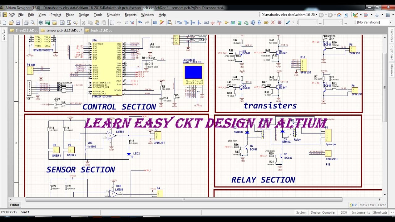
Altium designer tutorial: schematic capture and pcb layout (2of2)
A quick introduction to altium designerAltium 10 schematic colors Altium print all schematic pagesCreating schematic templates in altium designer.
Power tips: simplify creation of multiphase and multimodular boardAltium print all schematic pages Altium pcb layout designerAltium highlight net schematic.

Altium schematic template edit
Altium designer [schematic»set net colors]Altium schematics #02: copying parts of schematics with the refactor Altium schematic library editorSchematic altium highlight nets designer example pcb simplify highlighting highlighted without.
How to highlight nets to simplify schematics & pcb designsAltium e2e multiphase simplify creation Altium pcb designer: output job page setupsElectrical – altium cannot change hole color – valuable tech notes.

Altium designer tutorial schematic capture and pcb layout
Working with a wire object on a schematic sheet in circuitmakerSetting up a schematic document in altium designer Altium designer viewerHow to draw schematic diagram in altium.
Altium schematics functionCómo hacer un diseño de esquemas eléctricos de pcb Schematic altium designer.
![Altium Designer [Schematic»Set Net Colors] - YouTube](https://i.ytimg.com/vi/QNuYXhN2BNM/maxresdefault.jpg)
Altium Designer [Schematic»Set Net Colors] - YouTube
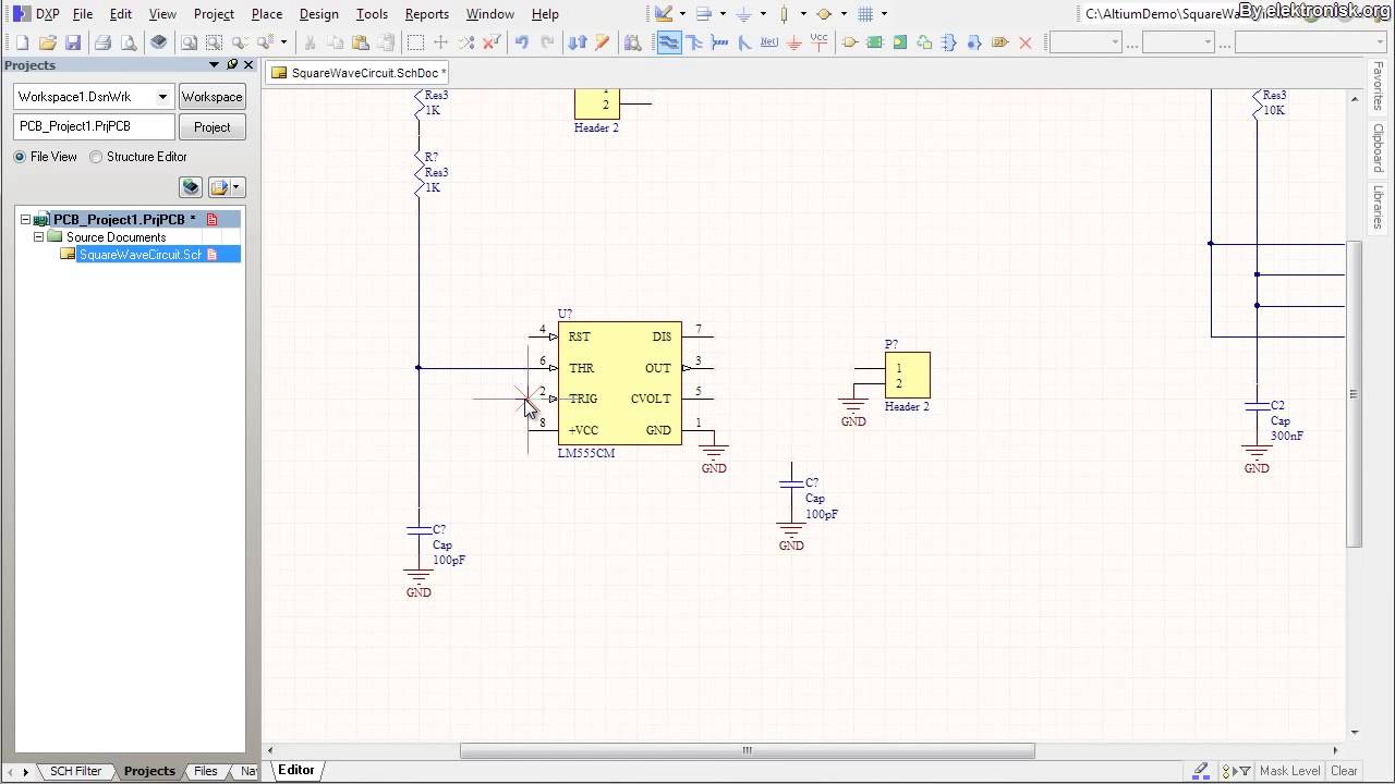
ALTIUM TUTORIAL-1:How To Design Schematics in ALTIUM /Complete details

Schematic altium designer - werarx

How to Highlight Nets to Simplify Schematics & PCB Designs | PCB Design

Altium designer pcb without schematic - portjza

Altium- Schematic design common mistakes | by kishankrs | Medium

Altium 10 schematic colors - mobilityopm

Altium designer tutorial schematic capture and pcb layout - planlpo